Jeroen's Project Journals
Audio amplifier
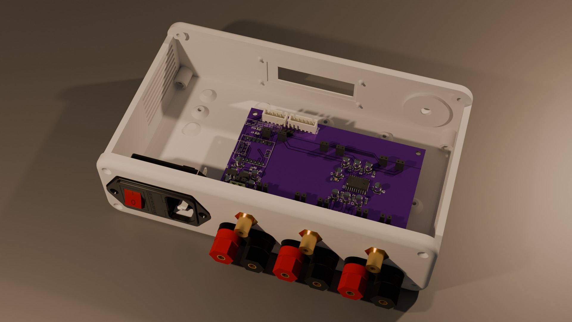
3-channel audio amplifier. Mains-powered and with digital volume control. Includes a 3D printed enclosure matching the Teensy DSP/DAC, OLED display and rotary click-encoder control
- Gallery
PCB works now!
2024-08-21
Success! Adding a level-shifter works as expected and the setup you see in the image below lets me control the volume of a single channel, and it actually sounds good:
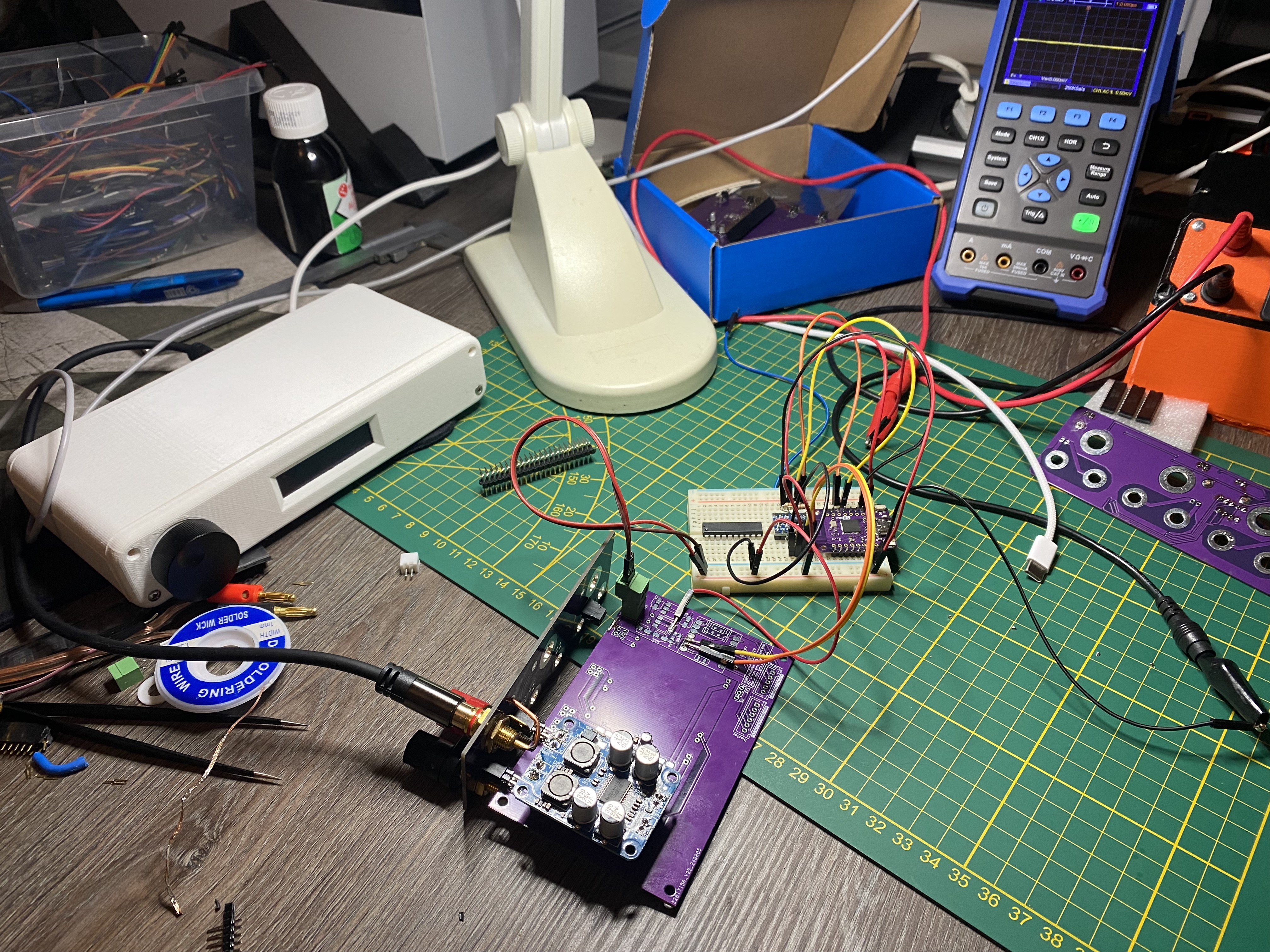 Initially I couldn’t get the PT2258 working at all though, and it took until the 4th chip before it worked. I probably have a batch of knock-offs or rejects. On the breadboard you can see the DIP-version of the PT2258 because I knew that worked before, so I wanted to check if there something wrong in my wiring or the PCB. But that one worked right away, so I tried another SOP-package, and that one did work.
Also, the connectors for the amplifier module are a bit janky. The power-in and speaker-out pads on the module are intended for a 3.81mm pitch connector, but there are no cheap, readily available 3.81mm pitch board-to-board connectors that are also height-compatible with the standard 2.54mm pitch pinheaders used for the mute and line-in pads. So I placed a 1-pin header at each contact point, which works but is not very sturdy. If I would redo the design I would change that to a single 3-pin 2.54mm header for both the power-in and speaker-out pads. The holes in the amplifier module are just large enough that 2 pins 5.08mm apart can fit through, with a bit of encouragement (a.k.a. “bending”).
So for now, all I need to do is wire up and mount the level-shifter on the PCB somehow. I’m thinking I will mount it on the bottom of the PCB using hot glue, which is where the I2C traces are. I can cut those traces, scrape away the solder mask in two places each and solder them to the HV and LV pins on the level-shifter.
An interesting aspect of this design is grounding. Ideally you want to keep the analog ground separate from the power and digital signal ground, but this may not be feasible. The PT2258 reference circuit interestingly distinguishes between AGND and DGND, but then connects them together. The PCB currently has split ground-planes, and I need to connect them to make things work (Maybe because they reference VCC to AGND?)
So IF I decide to change the design, here’s my todo-list:
- Change 3.81mm pitch pins for amplifier module to 3-pin 2.54mm header
- Modify location of power-connector, which currently interferes with one of the line-in connectors
- Integrate a level-shifter
- Connect AGND and DGND together
- (Maybe) improve routing of the analog signals to reduce interference
- (Maybe) make it a 4-layer board so I can better separate the digital and analog traces